
High Precision Positioners: Key Enablers in 3C and Semiconductor Manufacturing Applications
2025/04/23
With the rapid advancement of technology, the industrial customer's demand for high-precision, intelligent, and automated solutions is increasing rapidly. In light-load automation applications, high precision manual stages, micron-level motorized stages, and nanoscale stages have become indispensable core components of industrial intelligence due to their lightweight design, ease of use, and exceptional precision. These products not only effectively reduce labor costs but also address many instability factors in traditional production processes. They are widely used for precision displacement control in complex environments such as vacuum, non-magnetic conditions, and radiation-exposed settings.
Applications in 3C Products Manufacturing.
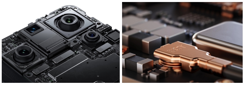
In the 3C (computer, communication, and consumer electronics) manufacturing industry, motorized stages play a crucial role in the production of mobile phones, computers, cameras, and other electronic devices. For example:
Precision machining of mobile phone casings
Screen bonding and camera installation
High-precision positioning and high-speed transmission
These applications significantly enhance production efficiency and product quality.
Based on the practical requirements of this field, Zolix has designed the CXP series motorized stages, which have been widely adopted by leading smartphone manufacturers and electronics producers. The CXP series features low-friction, wear-resistant guide rails and precision ball screw mechanisms with short screw pitch, ensuring high precision, durability, and full-size adaptability.
CXP series motorized stages
Travel range: 15-100mm
1mm screw pitch
Minimum incremental motion: 2um
Compact design
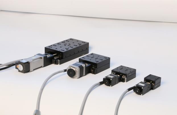
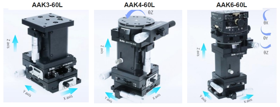
Applications in VR/AR Testing Manual Testing
Zolix Instruments provides 3 to 6 axes manual stages with sensitivity below 2µm. These stages can precisely position AR glasses at various pre-set test points to evaluate imaging distortion, resolution, screen defects, field of view (FOV), and other parameters.
Recommended products: AAK3-60L, AAK4-60L, AAK5-60L, AAK6-60L.
Applications in Optical Inspection
In applications such as aspherical mirror surface testing (e.g., measuring the flatness of semiconductor wafers or optical reflectors), the HXP-824 Series Hexapod provides six degrees of freedom for precise sample alignment.
HXP-824 Series Hexapod
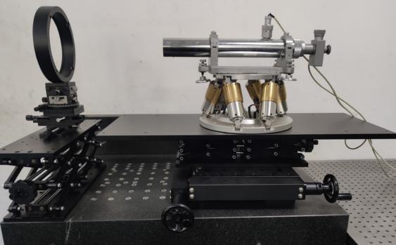
The HXP series six-axes parallel hexapod is designed for high-precision adjustments in 6 axes. It is especially suitable for applications such as spatial precision alignment, micro-component processing and assembly, lens inspection, optical communications, and motion simulation.
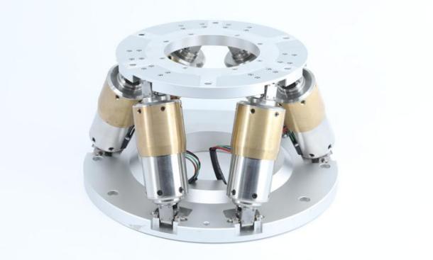
HXP–824A New models coming soon
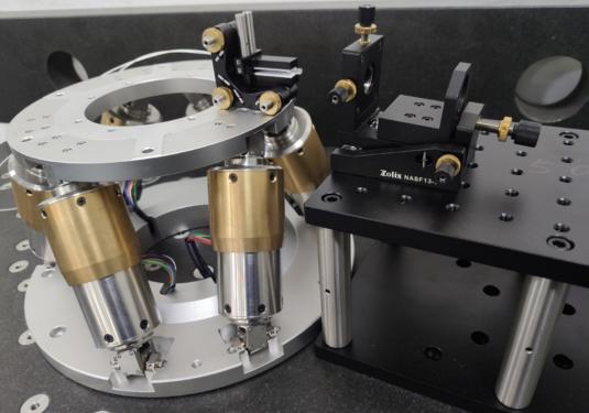
Applications in Optical Communication Component Alignment
A six-axes parallel robotic system assists in multi-dimensional alignment of optical communication components. By utilizing optical power feedback, it determines the optimal coupling position for maximum efficiency.
Nanometer-Level 6 Degree Freedom Parallel Platform
This platform can be adjusted at the nanoscale by piezoelectric actuator, making them ideal for wafer inspection and other nanotechnology applications.
Free6D.3-2.150.G2
Travel range:X, Y, Z ±10 mm, ±10 mm, ±5 mm
Angle range:ΘX, ΘY, ΘZ ±10 °, ±10 °, ±20 °
Minimum step size: 20 nm /1 urad
Multi-axis attitude adjustment, stable structure, high rigidity
High vacuum (.HV) and ultra High vacuum (.UHV) versions are available
Applications in Semiconductor Manufacturing
In semiconductor manufacturing, stage products are essential for wafer processing, chip assembly, wire bonding, and other critical steps. Piezoelectric stages are widely used in the semiconductor industry for material analysis of cast films, stretched films, optical materials, and electronic materials. Traditional motorized stages, which are bulky and less precise, can no longer meet the industry's stringent requirements. Piezoelectric stages, with their compact size and simplified structures, achieve nanometer-level precision positioning and motion control, significantly enhancing semiconductor manufacturing and inspection efficiency.
To address the demand for high-precision and compact motion control solutions, Zolix has developed a full range of products offering 1- to 6-axis precision motion control. For example, the S100.xyz.C/S200.xyz.C series are able to offer 1nm resolution motion in 3 axes. Utilizing advanced piezoelectric ceramic drive technology, these products offer ultra-high positioning accuracy, low noise, and excellent stability. They can be easily integrated into various precision equipment, meeting the stringent precision motion control requirements of semiconductor manufacturing, optical inspection, and material analysis.
S100.xyz.C
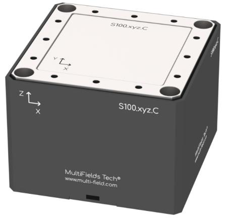
Closed loop resolution 1nm
Three dimensional XYZ motion maximum travel range 200 um x200 um x200um
Non-magnetic(.NM), high vacuum(.HV) and ultra-high vacuum (.UHV) versions are available.
Capacitive closed-loop sensor
Dimensions 55 mm x55 mm x40 mm
Applications in Microscopy & Inspection
Objective Lens Precision Positioning:
Zolix’s nanoscale focusing system is primarily used in semiconductor material inspection and electron microscopy.
Carrier.OB100.C
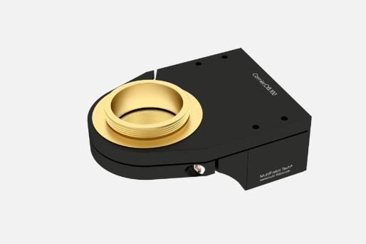
Z direction movement, travel range 50, 100 & 400um
Fast and stable movement, completed within 10ms
Support high load objective lens option; Provide a variety of objective lens transfer interface
Support third-party software and hardware control to achieve auto focus
The highest resolution reaches 0.2 nm
Non-magnetic (.NM), ultra-high vacuum (.UHV) versions are available.
Related products
MORE +-

DPbS series Room Temperature PbS Detectors
Room temperature IR detectors, spectral range from 0.8 to 3.2_m. DPbS2900 and DPbS3200 have the same construction (built-in pre-amplifier). -
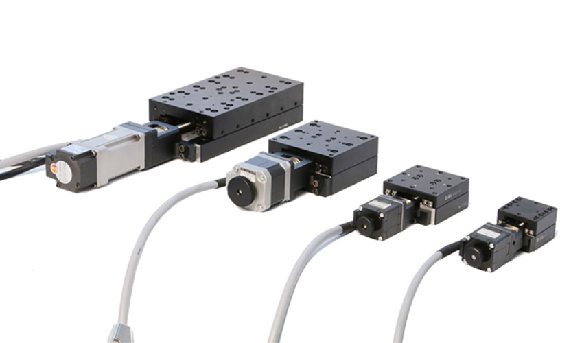
CXP and CXPF Series High-Precise Motorized Linear Stages
CXP series is special designed for the usage scenarios such as small-size and high frequency operation.The main body is made by hard aluminum alloy with black anodic-oxidation surface treatments which ensure the good wear resistance and nice appearance. -
.jpg)
AAK Series Combined Manual Stages
-
.jpg)
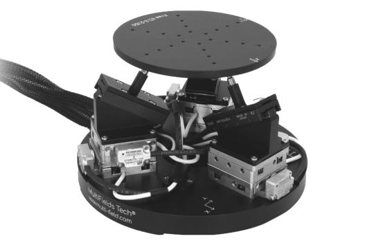
HXP High Precision Hexapod
HXP high precison hexapod is is mainly used for high-precision six-degree-of-freedom adjustment, and is particularly suitable for spacial precision alignment, micro-device processing and assembly, optical communication device core adjustment, wafer inspection and other occasions.